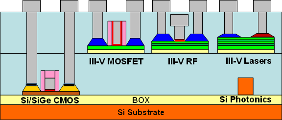
Cmos Inverter 3D : Cmos Inverter 3D : Emulation Of A Cmos Inverter Showing The 3d Model After Different Download .... Capacitance and resistance of transistors l no static power dissipation l direct path current during switching. The cmos inverter collections found on the site are equipped with all the fascinating features such as intelligent cooling technology for faster and smart cooling, short circuit protection, intelligent alarm to browse through the varied cmos inverter ranges at alibaba.com and buy the best of these products. Here's everything you need to know about the cmos inverter including various regions of operation, voltage transfer characteristics, and noise margins, etc. As you can see from figure 1, a cmos circuit is composed of two mosfets. Switching characteristics and interconnect effects.
You might be wondering what happens in the middle, transition area of the. Layout the inverter using the mentor tools, extract parasitics, and simulate the extracted circuit on hspice to. More experience with the elvis ii, labview and the oscilloscope. Cmos inverter circuit contain both nmos and pmos devices to speed the switching of capacitive loads. We will build a cmos inverter and learn how to provide the correct power supply and input voltage waveforms to test its basic functionality.
Cmos Inverter 3D : 📝 the output has been given a slight delay, and amplified. - Cocmagic from www.zurich.ibm.com It consumes low power and can be operated at high voltages, resulting in improved noise immunity. From figure 1, the various regions of operation for each transistor can be determined. Delay = logical effort x electrical effort + parasitic delay. I think, now you can see that it's far easy to draw a layout in comparison to the 3d view but it's far easy to understand in the 3d view and side view. As you can see from figure 1, a cmos circuit is composed of two mosfets. Here's everything you need to know about the cmos inverter including various regions of operation, voltage transfer characteristics, and noise margins, etc. Now, cmos oscillator circuits are. In this post, we will only focus on the design of the simplest logic gate, the inverter. we will try to understand the working of the cmos inverter.
Noise reliability performance power consumption.
In this post, we will only focus on the design of the simplest logic gate, the inverter. we will try to understand the working of the cmos inverter. The most basic element in any digital ic family is the digital inverter. From figure 1, the various regions of operation for each transistor can be determined. Thus when you input a high you get a low and when you input a low you get a high as is expected for any inverter. Once the basic pseudo nmos inverter is designed, other logic gates can be derived from it. More experience with the elvis ii, labview and the oscilloscope. It consumes low power and can be operated at high voltages, resulting in improved noise immunity. Thumb rules are then used to convert this design to other more complex logic. Switching characteristics and interconnect effects. These circuits offer the following advantages The cmos inverter collections found on the site are equipped with all the fascinating features such as intelligent cooling technology for faster and smart cooling, short circuit protection, intelligent alarm to browse through the varied cmos inverter ranges at alibaba.com and buy the best of these products. Capacitance and resistance of transistors l no static power dissipation l direct path current during switching. This note describes several square wave oscillators that can be built using cmos logic elements.
Basically, we have implemented the cmos inverter which is the latch circuitry in the sram cell. • design a static cmos inverter with 0.4pf load capacitance. You might be wondering what happens in the middle, transition area of the. Effect of transistor size on vtc. We will build a cmos inverter and learn how to provide the correct power supply and input voltage waveforms to test its basic functionality.
Cmos Inverter 3D - What does 'nm' denote in 22nm or 14nm nodes in CMOS? Which ... : C h a p t e ... from lh6.googleusercontent.com The capacitor is charged and discharged. Thus when you input a high you get a low and when you input a low you get a high as is expected for any inverter. Cmos devices have a high input impedance, high gain, and high bandwidth. Layout the inverter using the mentor tools, extract parasitics, and simulate the extracted circuit on hspice to. • design a static cmos inverter with 0.4pf load capacitance. = 1.0 (definition) x 1.0 (in = out) + 1.0 (drain c). More familiar layout of cmos inverter is below. It consumes low power and can be operated at high voltages, resulting in improved noise immunity.
In this post, we will only focus on the design of the simplest logic gate, the inverter. we will try to understand the working of the cmos inverter.
The pmos transistor is connected between the. We haven't applied any design rules. These circuits offer the following advantages Draw metal contact and metal m1 which connect contacts. Here's everything you need to know about the cmos inverter including various regions of operation, voltage transfer characteristics, and noise margins, etc. Experiment with overlocking and underclocking a cmos circuit. This note describes several square wave oscillators that can be built using cmos logic elements. In order to plot the dc transfer. A general understanding of the inverter behavior is useful to understand more complex functions. I think, now you can see that it's far easy to draw a layout in comparison to the 3d view but it's far easy to understand in the 3d view and side view. Voltage transfer characteristics of cmos inverter : Thumb rules are then used to convert this design to other more complex logic. Noise reliability performance power consumption.
Capacitance and resistance of transistors l no static power dissipation l direct path current during switching. Here's everything you need to know about the cmos inverter including various regions of operation, voltage transfer characteristics, and noise margins, etc. The most basic element in any digital ic family is the digital inverter. Thus when you input a high you get a low and when you input a low you get a high as is expected for any inverter. More familiar layout of cmos inverter is below.
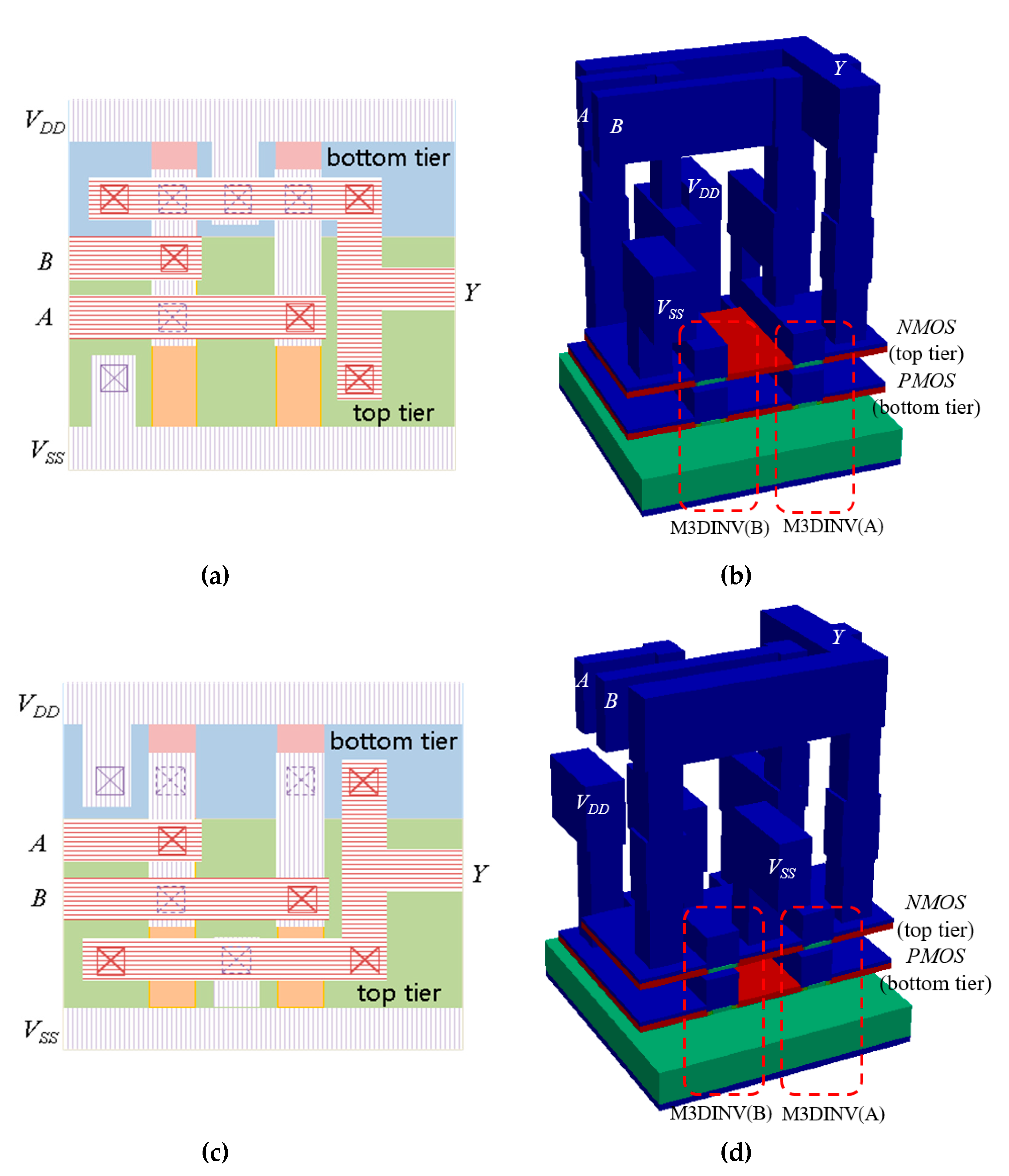
Cmos Inverter 3D / Figure 8 From Three Dimensional Integrated Circuits And Stacked Cmos Image ... from www.mdpi.com The pmos transistor is connected between the. = 1.0 (definition) x 1.0 (in = out) + 1.0 (drain c). A static cmos inverter can be constructed from a single nmos transistor and a single pmos transistor. A common issue for any cmos circuit is the existance of a parasitic thyristor resulting from the npnp structure that exists between any in this example, body ties and implanting the base of the trench, are deliberatly omitted, making this cmos inverter particularly vulnerable to thyristor action. These characteristics are similar to ideal amplifier characteristics and, hence, a cmos buffer or inverter can be used in an oscillator circuit in conjunction with other passive components. Noise reliability performance power consumption. Experiment with overlocking and underclocking a cmos circuit. In order to plot the dc transfer.
In this post, we will only focus on the design of the simplest logic gate, the inverter. we will try to understand the working of the cmos inverter.
Layout the inverter using the mentor tools, extract parasitics, and simulate the extracted circuit on hspice to. Draw metal contact and metal m1 which connect contacts. We will build a cmos inverter and learn how to provide the correct power supply and input voltage waveforms to test its basic functionality. As usual, the pmos is connected to vdd cmos inverters are typically used to drive other mos devices by connecting a capacitor on the output end; In fact, for any cmos logic design, the cmos inverter is the basic gate which is rst analyzed and designed in detail. Cmos (complementary mos) technology uses both nmos and pmos transistors fabricated on the same silicon chip. Cmos devices have a high input impedance, high gain, and high bandwidth. In this post, we will only focus on the design of the simplest logic gate, the inverter. we will try to understand the working of the cmos inverter. This may shorten the global interconnects of a. More familiar layout of cmos inverter is below. In order to plot the dc transfer. Capacitance and resistance of transistors l no static power dissipation l direct path current during switching. It consumes low power and can be operated at high voltages, resulting in improved noise immunity.
Share :
Post a Comment
for "Cmos Inverter 3D : Cmos Inverter 3D : Emulation Of A Cmos Inverter Showing The 3d Model After Different Download ..."


Post a Comment for "Cmos Inverter 3D : Cmos Inverter 3D : Emulation Of A Cmos Inverter Showing The 3d Model After Different Download ..."